Products utilizing High Bandwidth Memory (HBM) have thus far been few and far between but that isn't stopping Samsung and Hynix from pressing forward with development of a third generation.
At the Hot Chips conference in Cupertino, the two teased the aptly named HBM3 which looks to offer improvements all around. Best yet, it'll be much easier on the wallet which should hopefully translate to wider adoption by industry partners.

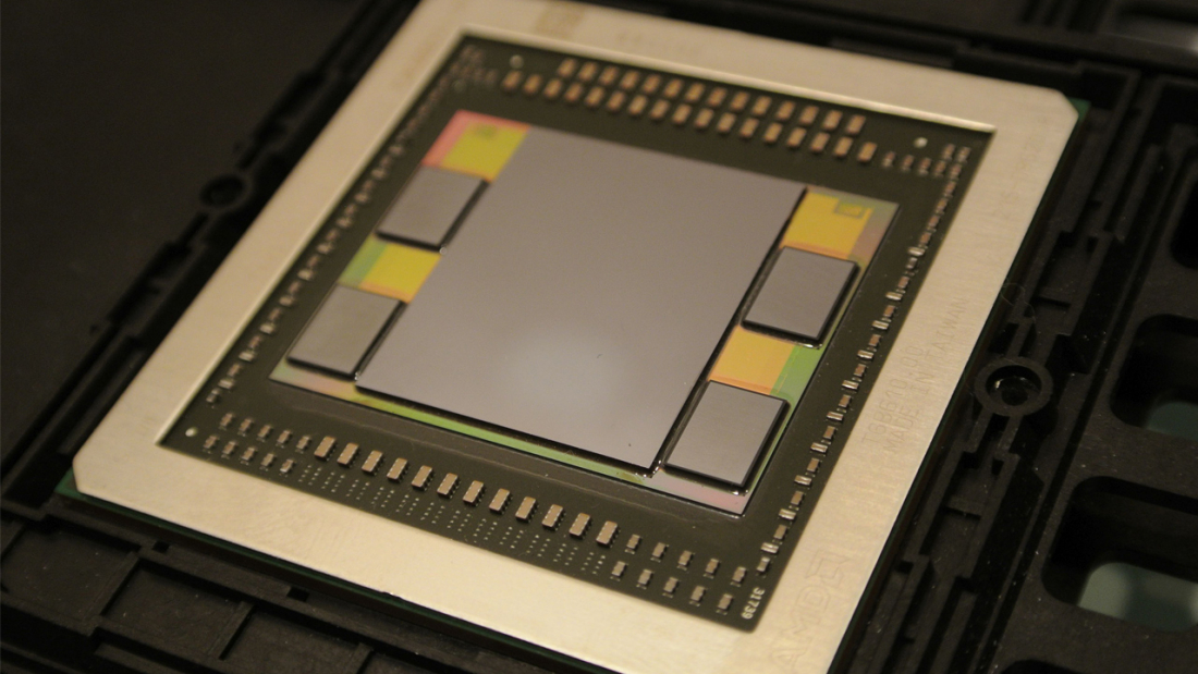
As Ars Technica explains, traditional memory setups consist of multiple RAM chips that are placed as close to the logic device (CPU or GPU) as possible. With HBM, however, memory is stacked on top of each other, connecting directly via through-silicon vias (TSVs). The stacked RAM is then placed on the logic chip package, a technique that reduces the physical real estate needed (think AMD's compact Fury Nano) and opens the door for massive bandwidth boosts.
Thus far, however, capacity and price have been the limiting factors to widespread adoption. Fortunately, these issues will be addressed with HBM3.
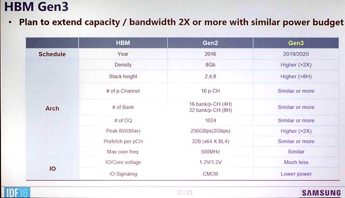
The third-generation technology will offer individual memory dies of 16Gb (up from 8Gb in HBM2) and allow more than eight dies to be stacked on top of each other. This means that video cards with as much as 64GB of memory will be possible. What's more, HMB3 will have a lower core voltage and twice the peak bandwidth (up to 512GB/s per layer of DRAM).
About the only "bad" news is that HBM3 won't be ready for another few years.
